Tandy 1110hd Bios Spelunking Part 2
Where We Left Off
We left of with my initial failure to get an XTA2SD card working in the Tandy 1110HD. I did get the Gotek functioning though so we had a means of booting the machine. So at least I knew that the motherboard appeared to be ok. No leaking caps, no blown fuses, just a dead floppy drive, dead battery, and no hard drive. Since then, I’ve made a few quality of life hardware changes that almost let me put the machine back together. If I weren’t still playing with the BIOS ROM adn the XTA2SD card, I’d probably have reassembled the machine by this point.
Working XTA2SD Without Patching the BIOS!
The original focus of this blog series was going to be digging through the BIOS of the machine to try to reverse engineer how it’s hard drive interfaces worked. We know it’s an XTA variant and that it is restricted to a very specific 20mb Conner drive. Since then, I’ve shipped one of the two machines I had to Germany and Callin has discovered the bit of magic needed to make his card work with the stock BIOS!
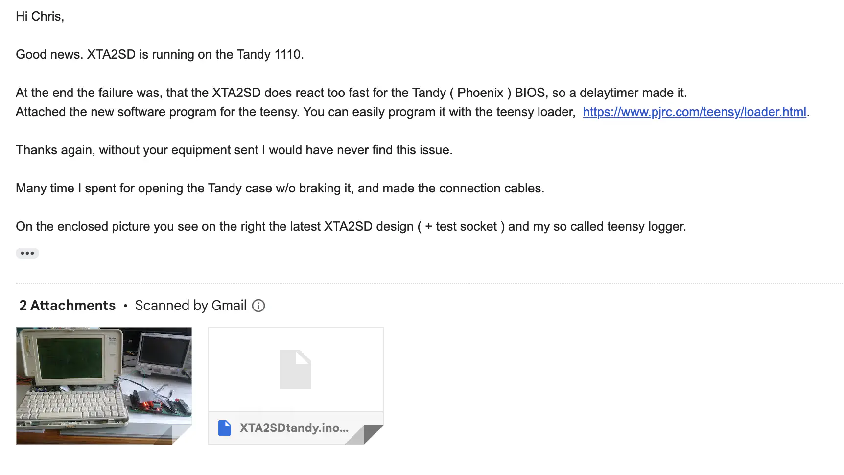
He got it working!
It turned out to a simple timing issue that was easy to resolve once the hardware was available! Quick firmware upgrade, and I’ve got a working machine! Callin is also working on a board that actually fits the mount points inside the Tandy 1110HD case and with better component positioning for the restricted environment. I’m waiting to get my hands on a prototype to play with. Screw mounting will be much better than my current double side tape solution. This version will also work with stock cable! So no more hand adapting ribbon cables to an IDC (insulation displacement connector).
I have no idea what the availability on this card will be, so keep an eye on the thread in the VCF forum for updates.
Quality of Life Changes.
In the last post, I showed mounting the Gotek board inside the case. Since I didn’t want to cut a massive hole in the side of the machine and potentially compromise its structural integrity to fit the stock Gotek case, I ditched the Gotek’s plastics. There’s nothing particularly special about those plastics since the Gotek board has no mechanical components to it. Unfortunately, that does leave the USB connector and display in somewhat awkward locations inside the machine. There’s a metal cage that’s meant to hold the stock floppy drive and battery.
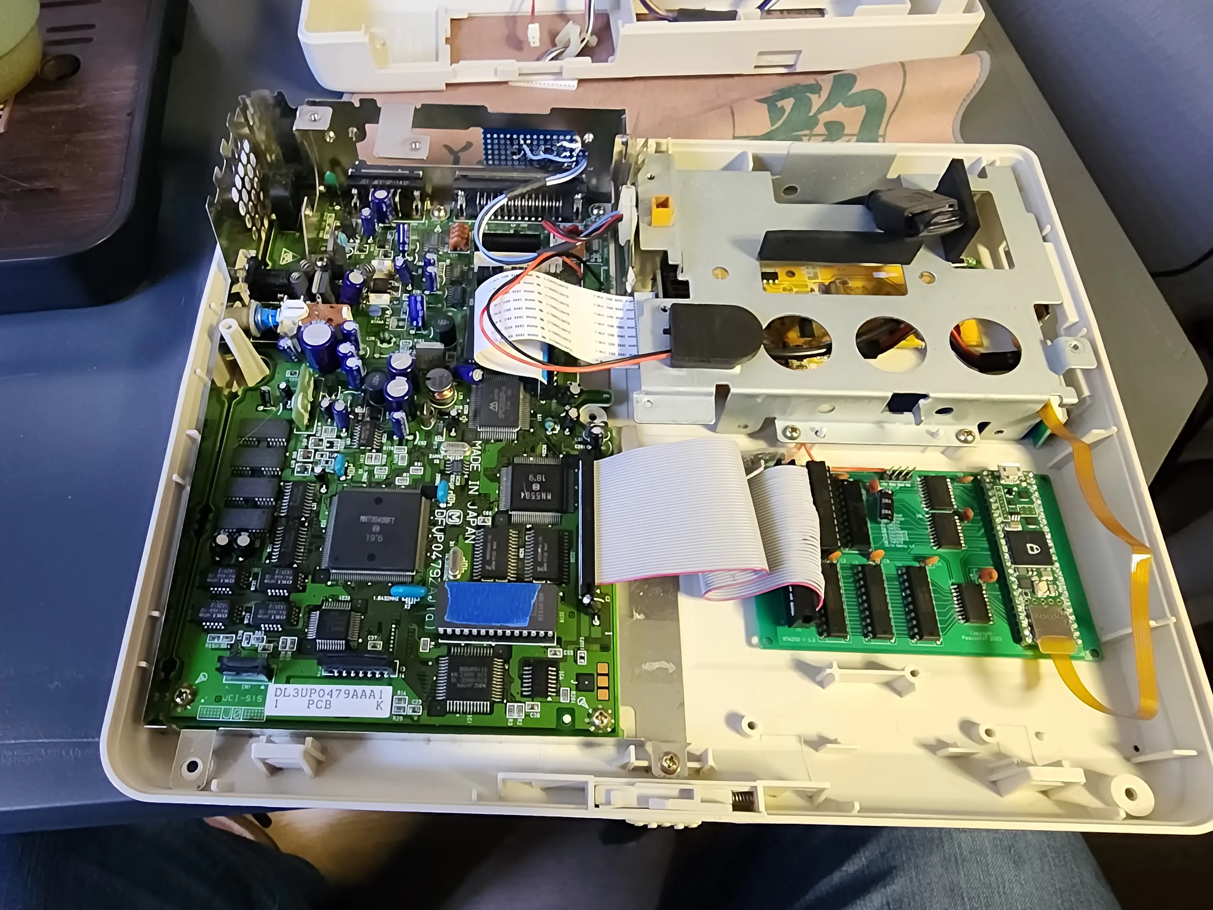
Interior view of the Tandy 1110HD showing the floppy mounting cage.
In the picture, I have the metal frame in place with a USB extension connector sticking up through an existing hole in the battery compartment. There’s enough length that can feed this through to the expansion slot on the back, which is how I have it setup right now. It’s a little awkward just flopping around but it’s way better than having to take the machine completely apart the change out the flash drive and load it with new images.
The part I found is a female USB pigtail with bare leads. My only complaint is that I had to trace which pins went to which leads before soldering it to the Gotek. I could have left the original connector in place on the Gotek board, but I decided to remove it and just wire up the pigtail instead. The Gotek is going to be a permanent fixture in this machine anyhow, so there’s no point in maintain its original configuration.
I’ll reiterate my recommendation to use FlashFloppy on any Gotek board that will support it and disregard ones that don’t. The stock firmware works, but is so annoying to work with as to be almost unusable. I’ll add that you want an OLED display on your Gotek board if you can get it. Mine didn’t come with one, but I had a few spares laying around from building a couple of custom keyboards. It’s surprisingly easy to wire one up and replace the LED display. Both displays use a similar serial interface and only need four wires (Data, Clock, Vcc, and Ground) to get working.
The main difference is that the OLED enables certain operations that don’t appear to be available with the LED display. In particular, the ability to copy images on the drive and to see the file names of the images you’re working with. The indexed display you get with the LED is ok, it will work, but you’re leaving a bunch of functionality on the table. They’re also cheap to parts.
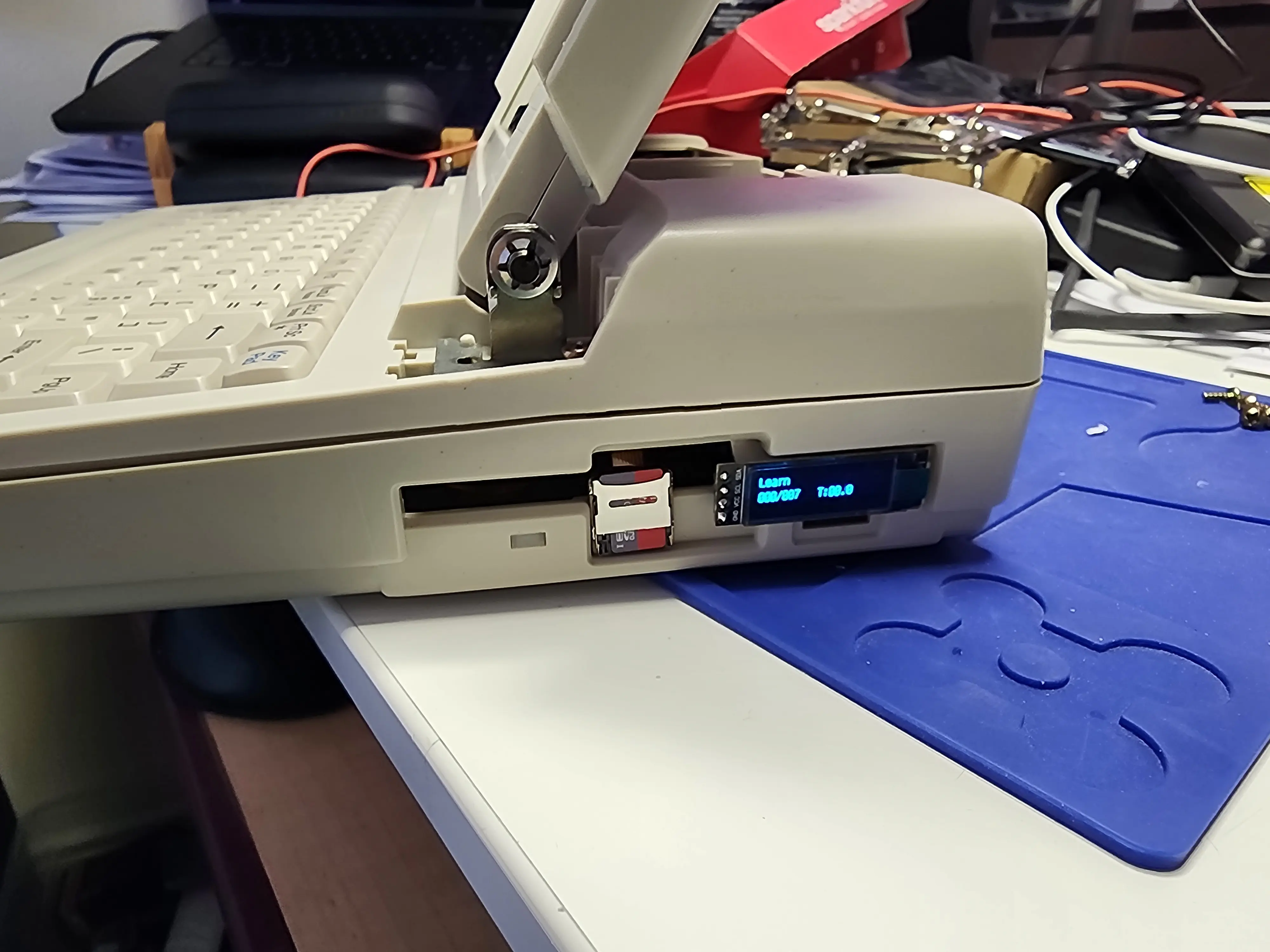
OLED display for Gotek temporarily mounted.
SD Card Extension … Just Don’t
This one, I’ll have to recommend against. I found a couple of promising looking adapters that would let me extend the SD-Card socket so it wouldn’t be hidden away under the keyboard. The one that was long enough worked for all of a couple of hours before failing. I’m not sure why or even how. I’m guessing it was either not well shielded enough or the Teensy can’t drive the SD-Card correctly through the longer wires but it stopped working. Thankfully, everything started functioning again once I pulled the extension and slotted the SD-Card into the Teensy directly.
Now for the BIOS
Now for the fun part. At heart, I’m a software guy. The hardware stuff is kind of interesting but not something I’m very good at or have a lot of expertise in. What I do have a bit of background in is code and digging around in somewhat legacy systems trying to figure out why bits and bobs do what they do, though usually not to the point of reverse engineering software I don’t have sources to. That makes this a bit of a challenge, especially considering that a number of the tools in this space are expensive, particularly if you want a specific architecture.
After a few attempts, I settled on Ghidra as my tool of choice. There were others I looked at but they either didn’t allow for tweaking the disassembly based on things I’d learned about the code, didn’t cover the architecture I wanted (16bit real mode assembly for the 8088/8086), or would have cost me an arm and a leg. Since this is a hobby exercise and not a professional gig, I couldn’t conscience spending what it looked like I’d need to on the other offerings. So Ghidra it is.
Thankfully, the Tandy 1110HD ROM is socketed and a standard 27C256 IC. Both examples I’ve examined use the same code, though I can’t say that all of them do. Thankfully Jameco Electronics had AM27C256 in stock so I picked up ten of them. Since this is a UV erasable EPROM, I wanted to be able to iterate faster than the erase time on the EPROM and I’d never dealt with UV EPROMs before only flash.
With a flash EEPROM, there is no wait time, erasing is as fast as your programmer can write to the chip. UV ERPROMs require exposure to particular wavelengths of UV light for some period of time to clear the chip. For my chips and lamp, it takes about 20 minutes to ensure the chip is fully erased, which is a heck of a time to add to your development cycle. With 10 chips, I could burn one, put it in the machine, test and iteration, yank it and add it to the erase tray and still have a spare to burn almost immediately. The test/dev cycle time was enough that I could have gotten by with 5 chips, but spares never hurt and they weren’t that expensive. I’ll likely find other uses for them down the road as well.
I’ll warn you, I am by no means an expert with Ghidra and have likely gone about this in all the wrong ways. There’s probably a much easier/better way to the result I’m looking for that isn’t quite as brute force, but what little I know has worked. Through a combination of lots and lots of Google searching and tracing 16bit real mode assembly, something I haven’t messed with in decades and was never really that good at, I’ve picked up a lot about this machine.
Some CPU Basics
The Tandy 1110HD uses an NEC V20 as a cpu which is pin and software compatible with the Intel 8088. The V20 is slightly more efficient and adds a few instructions from the 80186. It’s also a touch more efficient allowing it to execute more instructions for a given unit of time than the 8088 at the same clock speed. For our purposes, the chip can be treated identically to the 8088 though.
To boot, 8088/8086 chips jump to a fixed address at the very bottom of the address space. The chip itself uses a 20bit address but provides two 16bit values to represent addresses to programmers: a segment address and an offset address. To get the physical 20bit address segment addresses are shifted to the right by 4 bits and added to an offset address. This breaks the available memory down into a set of 64k windows, unsurprisingly called segments, that can overlap. There are four segment registers:
- CS - Defines the code segment with CS:IP pointing to the instructions.
- SS - Defines the stack segment with SS:SP pointing to the top of the stack.
- DS - Defines the data segment where most memory read/write operations happen. DS:DI and DS:SI are used for string and copy operations etc.
- ES - Defines an extra segment for general purpose usages.
This gives rise to the concept of a near and far pointer that doesn’t really exist in flat, unsegmented, memory models. Far pointers including a segment address to allow pointing to memory outside or the current segment.
Boot Process
At start up, the 8088 executes a far jump to a reset vector at FFFF:0000, near the very top of ram. That address leaves about 16 bytes for an instruction which is usually a trampoline to the real BIOS start up routines.

Ghidra screen shot of the reset vector.
If you look at the screen shot, there are a couple of things that become immediately apparent. I said the reset vector was FFFF:0000 but the screen shot shows a JMPF at F000:FFF0 which, on face, does not quite line up. This is mostly because of how I had the origin configured when I let Ghidra initially analyse the code. Because of the way segment addressing works F000:FFF0, FF00:FF00, FFF0:F000, and FFFF:0000 all point to the same FFFF0 20bit address even though they look different. This is one of those fun little tidbits that’s easy to get tripped up on.
There’s several other things here as well, including a date code and something I’ve labeled as a System_Model. When Ghidra analyses code, it places generic labels on things that reference the address and a type of access to that location in memory. Thankfully, it let’s you rename those labels as you go. So any non-generic labels in the examples are mine and purely guesses based on my understanding of the code or research. These come from online research about standardized bios entry points. There’s a nice listing of some of them in Sergey Kiselev’s 8088 Bios repo over on Github.
For our example, the reset vector jumps to another trampoline jump instruction at F000:E05B. There isn’t a technical reason in the code itself that requires this extra jump other than applications in the wild seem to expect it.
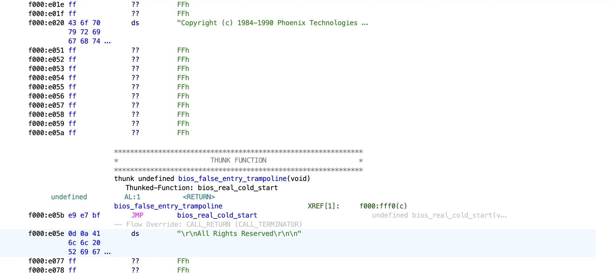
Ghidra screen shot of standard entry point.
There are also copyright notices hiding randomly in the code for this bios, spread out all over the place to confuse things. String values cause all kinds of fun with disassemblers since they aren’t always immediately recognizable as strings instead of instructions. This can cause incorrect disassembly, which is relatively easy to correct but requires manual handling.
After those two jumps, we get to the real bios cold start routines at F000:A045. First, disabling interrupts, we haven’t setup the interrupt vectors yet so that makes sense, and then a slew of writes to various I/O ports. Most of these weren’t, or at least did’t appear to be related to what I was working of so I skimmed over them. The I/O ports use the same address and data bus lines on CPU (though I believe only 16bits of addressing are available for I/O ports) and a separate control line to indicate that a RAM or I/O operation is occurring. What these I/O ports represent is pretty well documented on line if your interested in looking them up.
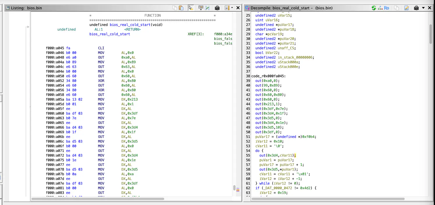
Ghidra screen shot of i/o port operations with equivalent decompilation.
OUT and IN are the two instructions (or family of instructions) that the 8088 series chips use to write to I/O ports. There are a couple of variants with depending on the size of the operands and port number. For port numbers that fit in 8bits the port number can be specified as an immediate. Large ports require specifying the port number in a register. Since the data bus is 8bits, all values sent or read are limited to 8bits.
Write to low port:
    mov al, 0x0
    out 0xa0, al
Write to high port:
    mov dx, 0x3d5
    mov al, 0x0
    out dx, al
XTA hard drive interfaces live on three ports starting at 320 hex. So none of these are what we’re interested in. There’s a bunch of code here that I skimmed over for a while before giving up on the instruction by instruction trace and started looking for interesting values. A ways down at F000:A6A1 I found the string “Diskette drive 0 seek failure” which I know happens right after attempting to spin up the hard drive.
An Aside About C-Strings
This is another little tidbit of interesting code:

Example of novel c-string output function.
This functions is used all over the bios to write c-strings (also known as ascii-z or null terminated strings) to the display. There’s no setup code, just a call and a null terminated string immediately following it. The first few examples of this I came across caused problems with the disassembler because the ascii characters looked like part of an instruction. To fix this, highlight the region, right click, and select “Clear Code Bytes” in Ghidra. Then select the bytes that represent the string and decode them as a “Terminated CString”. Then you can re-analyse the selected region to find that call.
The function itself uses the return address from the stack to find the string, output it, and then updates the return address to return after the instruction after the string. It’s actually a pretty ingenious little trick.
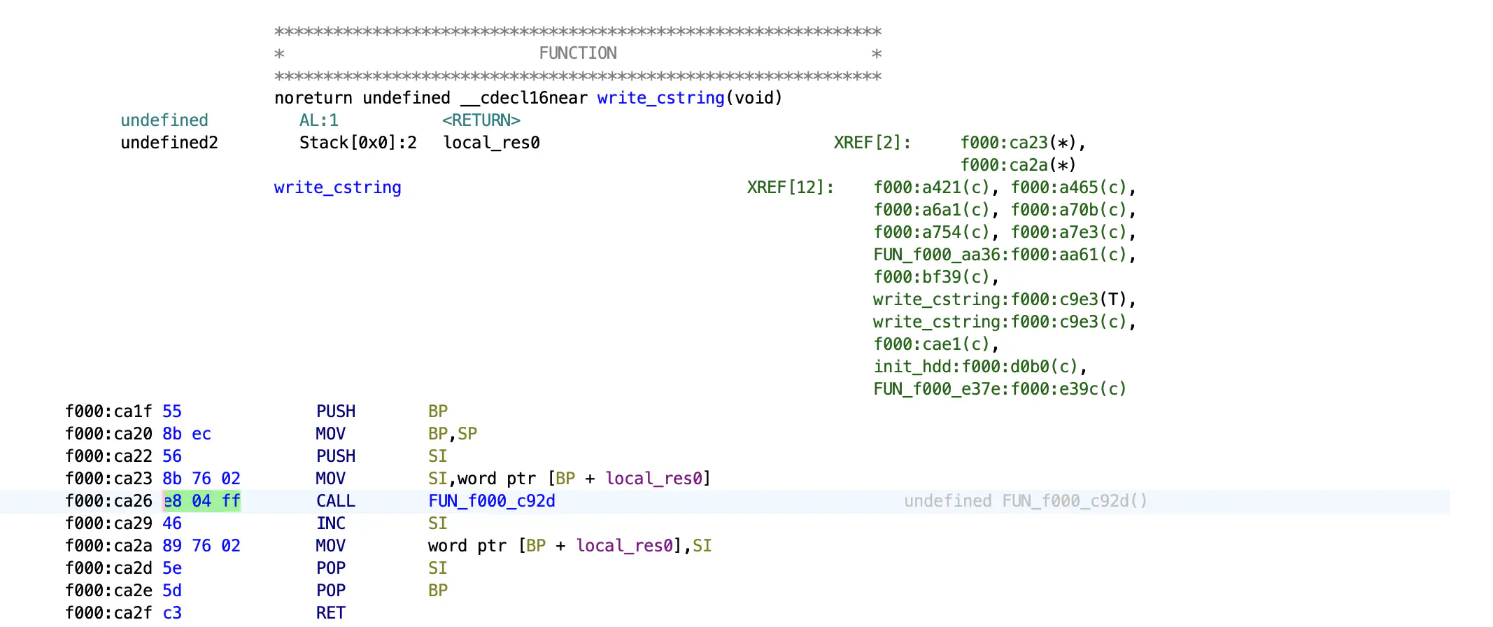
Ghidra screen shot of c-string functon.
In this screen shot, you’ll notice that the move instruction at F000:CA26 references a local_res0 that Ghidra calls undefined. I think this is an artifact of the decompilation process. There are a number of online disassemblers that can handle hex encoded machine code pretty well. If we take that snippet and drop it into one it comes back with:
0x0000000000000000:  55          push bp
0x0000000000000001:  8B EC       mov  bp, sp
0x0000000000000003:  56          push si
0x0000000000000004:  8B 76 02    mov  si, word ptr [bp + 2]
0x0000000000000007:  E8 04 FF    call 0xff0e
This clearly shows that local_res0 is a constant of 2. I’m pretty sure this code is using the treating the stack and data segments as the same value so bp + 2 is the second value down in the stack. Our first instruction was to push bp so the second value down is the return address form the call. From the Ghidra disassembly, the code jumps off into the actual write routines, that I didn’t dig into and returns with si having been updated to point at the null terminator. This wrapper, updates the return address, cleans up it’s stack frame and returns to right after the inline string. Ingenious.
Hard Drive Init Routines
If you backtrack from that code a bit we find an int 13h call, which is a disk interrupt, and some references to option ROM address. I think I actually started searching for the 320h scalar value hunting for writes to the hard drive controller ports to actually find this code, but I’ve slept since then and don’t remember exactly how I traced it out. Ghidra can trace where addresses are referenced pretty easily once it’s analyzed the code so there were portions of this I traced by following the instructions and others I backtracked by looking at what referenced particular labels.
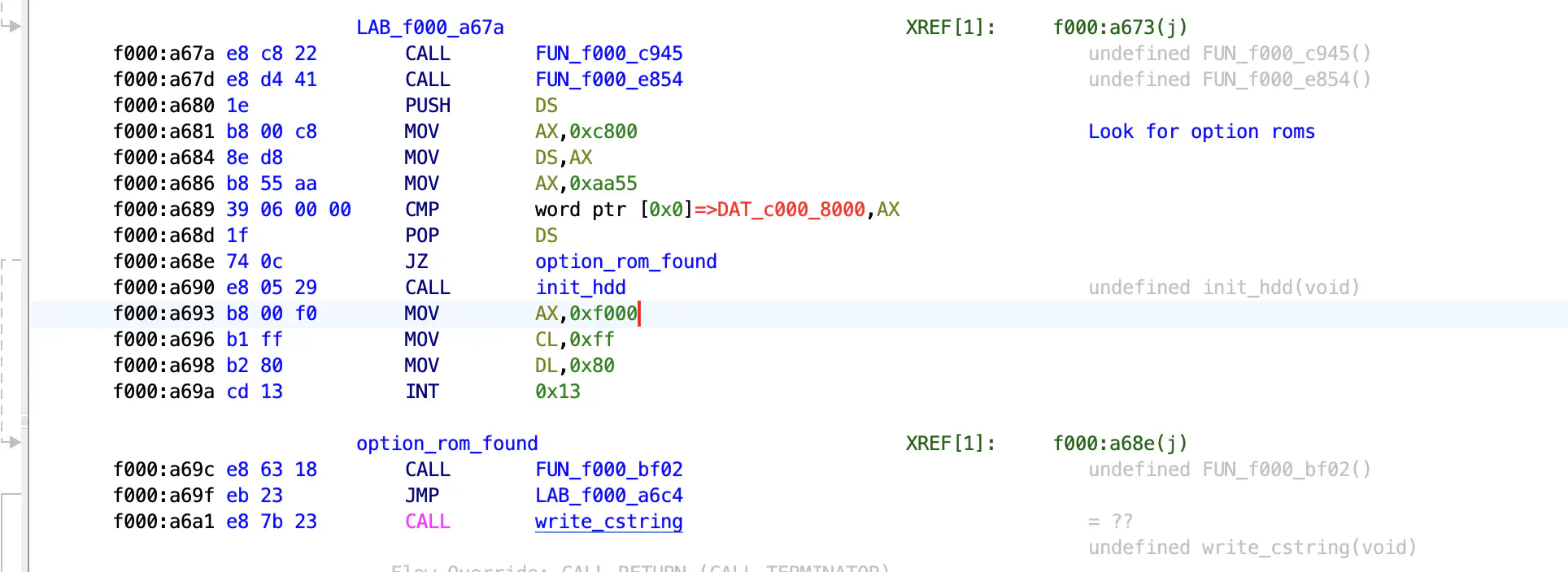
Ghidra screenshot of init_hdd function call.
I think I actually started searching for the 320h scalar value hunting for writes to the hard drive controller ports to actually find this code, but I’ve slept since then and don’t remember exactly how I traced it out. Ghidra can trace where addresses are referenced pretty easily once it’s analyzed the code so there were portions of this I traced by following the instructions and others I backtracked by looking at what referenced particular labels.
This is definitely where we want to be though. Unfortunately, this post is getting a bit long, so I’m going to cut off here and leave dissecting the init_hdd function until next time.
See you then!